Isolator-integrated photonics chip reduces back-reflected light approximately 95%, enabling faster, energy-efficient AI data centers
Kyocera Corporation (President: Shiro Sakushima; "Kyocera") and the Research Institute of Electrical Communication (RIEC), Tohoku University (Director: Kazushi Ishiyama; "Tohoku University") have developed a new technology*1 for integrating optical isolators onto silicon photonics chips using "laser annealing," a localized, laser-based heat-treatment method.
An optical isolator is a component that stabilizes optical communication by allowing optical signals to be transmitted in only one direction, reducing signal reflection.
A paper summarizing these results was published on Sep. 2, 2026, in "IEEE Access," an academic journal issued by the Institute of Electrical and Electronics Engineers (IEEE).
This press release features multimedia. View the full release here: https://www.businesswire.com/news/home/20260910368647/en/
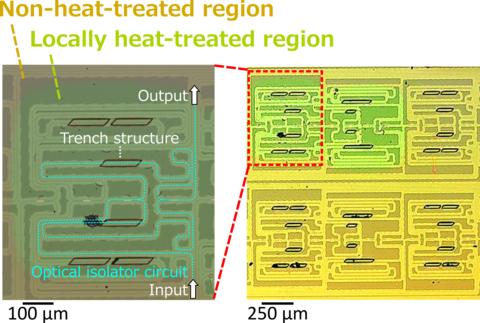
Microscopic image of the optical isolator fabricated and integrated onto a silicon photonics circuit by laser annealing
*1 |
For technology that integrates an optical isolator into a silicon photonics circuit using a laser annealing method; according to Kyocera research, July 2026. |
Development Background
As generative AI and related technologies place unprecedented demand on global data networks, silicon photonics*2 offers a solution for faster and more energy-efficient data centers. The expansion of silicon photonics is fueling demand for technologies enabling Co-Packaged Optics (CPO), which integrate optical and electronic circuits within the same semiconductor package to minimize signal paths, signal loss and power consumption.
In optical circuits, light reflected back into the laser light source degrades performance. Optical isolators, which suppress reflected light, can overcome this challenge. The next generation of compact, integrated optical circuits incorporating CPO technology will require optical isolators that can be fabricated directly onto silicon photonics chips.
Optical isolators typically use a crystalline material known as “magneto-optical garnet.” To function as an optical isolator, this material requires heat treatment at approximately 600°C or higher. However, heating the entire silicon photonics chip to this temperature can damage electrodes, wiring and other on-chip elements. Finding a way to selectively heat-treat only the magneto-optical garnet without overheating other areas of the chip has remained a significant challenge.
To address this challenge, Kyocera and Tohoku University developed a monolithic integration technology*3 that directly fabricates optical isolators onto silicon photonics chips through a “laser annealing” process, in which a laser beam is applied locally to the areas of the chip requiring heat treatment. Kyocera and Tohoku University demonstrated the device’s operation.
*2 |
Silicon photonics: A technology that forms optical circuits on silicon, a semiconductor material, and uses optical instead of electrical signals to transmit and process information. |
*3 |
Monolithic integration technology: A technology that integrally forms multiple functional elements on the same substrate. |
Features
1) Localized laser heating enables heat treatment of magneto-optical garnet without damaging the silicon photonics chip
A near-infrared laser beam is applied only to an optical isolator circuit region measuring approximately 700x700 microns (μm), where the magneto-optical garnet film has been deposited, causing it to crystallize with the properties needed to suppress reflected light. Unlike conventional methods that heat the entire chip in a furnace, this approach virtually eliminates thermal impact on the surrounding optical circuits and electrodes.
2) Optical isolator test on silicon photonics chip
Using this technology, the research team fabricated a device with a structure that utilizes light interference and experimentally demonstrated its operation as an optical isolator. In the experiment, the team compared the optical output corresponding to signal light, or forward propagation, with that corresponding to back-reflected light, or backward propagation. The results confirmed an isolation ratio of 13.6 dB in the optical communication wavelength range, reducing back-reflected light by approximately 95%. Electron microscopy also confirmed that the magneto-optical garnet in the laser-irradiated area had crystallized well on the silicon waveguide.
Future Development
Kyocera and Tohoku University have previously worked together to develop related optical isolator technologies that can be integrated onto optical circuits*4. To commercialize these technologies, the two organizations aim to achieve even lower loss, higher efficiency and improved productivity for mass production. They will continue to advance their collaboration and contribute to the development of an efficient and sustainable information society.
*4 |
Prior joint research result (T. Sugita et al., “Nanocomposite Garnet-Enabled Monolithically Integrated Magneto-Optical Isolator Using an Asymmetric Mach–Zehnder Interferometer,” ACS Appl. Opt. Mater., vol. 4, no. 6, pp. 1813–1820, Jun. 2026, doi: 10.1021/acsaom.6c00176). |
Paper Information
Journal: IEEE Access
Title: Monolithic Magneto-Optical Mach–Zehnder Isolator Using Laser-Annealed Iron Garnet on a Silicon Waveguide
Authors: Tomoya Sugita, Reona Motoji, Yuki Yoshihara, Dan Maeda, Hiroki Yamamoto, Hibiki Miyashita, Kazushi Ishiyama, Taichi Goto
DOI: 10.1109/ACCESS.2026.3729586 (https://doi.org/10.1109/ACCESS.2026.3729586)
- IEEE is a registered trademark of The Institute of Electrical and Electronics Engineers, Incorporated.
View source version on businesswire.com: https://www.businesswire.com/news/home/20260910368647/en/
Contacts
KYOCERA Corporation (Japan) Corporate Communications
Head Office TEL: +81-(0)75-604-3514 E-mail: webmaster.pressgl@kyocera.jp
RIEC Public Relations Office, Tohoku University
Tel: +81-(0)22-217-5427