As of late 2025, the artificial intelligence revolution has reached a critical inflection point where the speed of silicon is no longer the primary constraint. Instead, the industry’s gaze has shifted to the "Memory Wall"—the physical limit of how fast data can move between a processor and its memory. High Bandwidth Memory (HBM) has emerged as the most precious commodity in the tech world, serving as the essential fuel for the massive Large Language Models (LLMs) and generative AI systems that now define the global economy.
The announcement of Nvidia’s (NASDAQ: NVDA) upcoming "Rubin" architecture, which utilizes the next-generation HBM4 standard, has sent shockwaves through the semiconductor industry. With HBM supply already sold out through most of 2026, the competition between the world’s three primary producers—SK Hynix, Micron, and Samsung—has escalated into a high-stakes battle for dominance in a market that is fundamentally reshaping the hardware landscape.
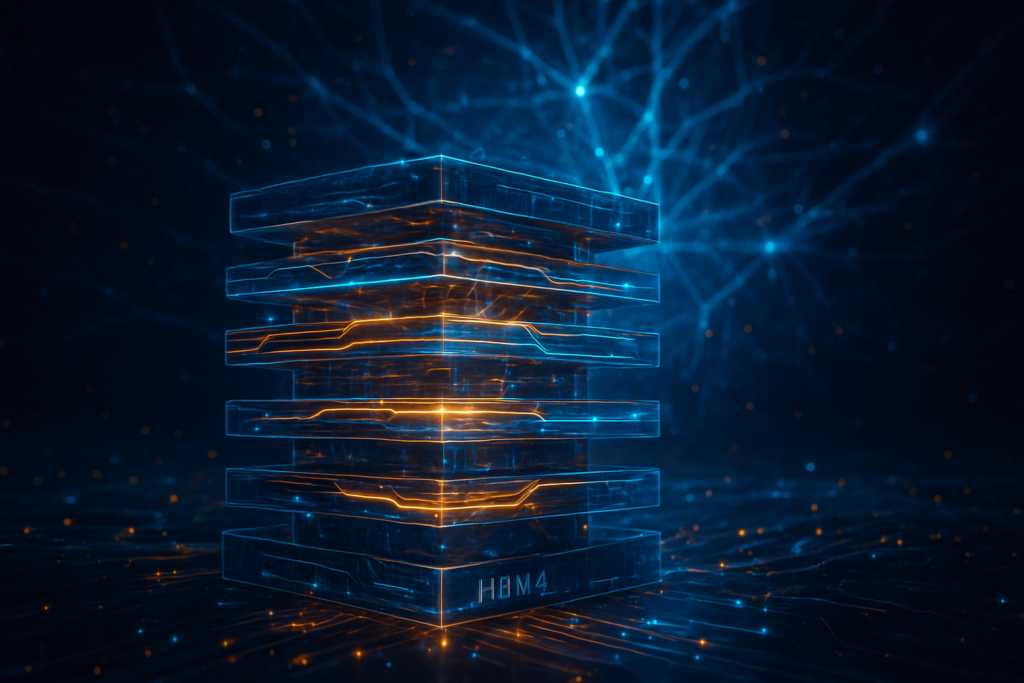
The Technical Leap: From HBM3e to the 2048-bit HBM4 Era
The technical specifications of HBM in late 2025 reveal a staggering jump in capability. While HBM3e was the workhorse of the Blackwell GPU generation, offering roughly 1.2 TB/s of bandwidth per stack, the new HBM4 standard represents a paradigm shift. The most significant advancement is the doubling of the memory interface width from 1024-bit to 2048-bit. This allows HBM4 to achieve bandwidths exceeding 2.0 TB/s per stack while maintaining lower clock speeds, a crucial factor in managing the extreme heat generated by 12-layer and 16-layer 3D-stacked dies.
This generational shift is not just about speed; it is about capacity and physical integration. As of December 2025, the industry has transitioned to "1c" DRAM nodes (approximately 10nm), enabling capacities of up to 64GB per stack. Furthermore, the integration process has evolved. Using TSMC’s (NYSE: TSM) System on Integrated Chips (SoIC) and "bumpless" hybrid bonding, HBM4 stacks are now placed within microns of the GPU logic die. This proximity drastically reduces electrical impedance and power consumption, which had become a major barrier to scaling AI clusters.
Industry experts note that this transition is technically grueling. The shift to HBM4 requires a total redesign of the base logic die—the foundation upon which memory layers are stacked. Unlike previous generations where the logic die was relatively simple, HBM4 logic dies are increasingly being manufactured on advanced 5nm or 3nm foundry processes to handle the complex routing required for the 2048-bit interface. This has turned HBM from a "commodity" component into a semi-custom processor in its own right.
The Titan Triumvirate: SK Hynix, Micron, and Samsung’s Power Struggle
The competitive landscape of late 2025 is dominated by an intense three-way rivalry. SK Hynix (KRX: 000660) currently holds the throne with an estimated 55–60% market share. Their early bet on Mass Reflow Molded Underfill (MR-MUF) packaging technology has paid off, providing superior thermal dissipation that has made them the preferred partner for Nvidia’s Blackwell Ultra (B300) systems. In December 2025, SK Hynix became the first to ship verified HBM4 samples for the Rubin platform, solidifying its lead.
Micron (NASDAQ: MU) has successfully cemented itself as the primary challenger, holding approximately 20–25% of the market. Micron’s 12-layer HBM3e stacks gained widespread acclaim in early 2025 for their industry-leading power efficiency, which allowed data center operators to squeeze more performance out of existing power envelopes. However, as the industry moves toward HBM4, Micron faces the challenge of scaling its "1c" node yields to match the aggressive production schedules of major cloud providers like Microsoft (NASDAQ: MSFT) and Google (NASDAQ: GOOGL).
Samsung (KRX: 005930), after a period of qualification delays in 2024, has mounted a massive comeback in late 2025. Samsung is playing a unique strategic card: the "One-Stop Shop." As the only company that possesses both world-class DRAM manufacturing and a leading-edge logic foundry, Samsung is offering "Custom HBM" solutions. By manufacturing both the memory layers and the specialized logic die in-house, Samsung aims to bypass the complex supply chain coordination required between memory makers and external foundries like TSMC, a move that is gaining traction with hyperscalers looking for bespoke AI silicon.
The Critical Link: Why LLMs Live and Die by Memory Bandwidth
The criticality of HBM for generative AI cannot be overstated. In late 2025, the AI industry has bifurcated its needs into two distinct categories: training and inference. For training trillion-parameter models, bandwidth is the absolute priority. Without the 13.5 TB/s aggregate bandwidth provided by HBM4-equipped GPUs, the thousands of processing cores inside an AI chip would spend a significant portion of their cycles "starving" for data, leading to massive inefficiencies in multi-billion dollar training runs.
For inference, the focus has shifted toward capacity. The rise of "Agentic AI" and long-context windows—where models can remember and process up to 2 million tokens of information—requires massive amounts of VRAM to store the "KV Cache" (the model's short-term memory). A single GPU now needs upwards of 288GB of HBM to handle high-concurrency requests for complex agents. This demand has led to a persistent supply shortage, with lead times for HBM-equipped hardware exceeding 40 weeks for smaller firms.
Furthermore, the HBM boom is having a "cannibalization" effect on the broader tech industry. Because HBM requires roughly three times the wafer area of standard DDR5 memory, the surge in AI demand has restricted the supply of PC and server RAM. As of December 2025, commodity DRAM prices have surged by over 60% year-over-year, impacting everything from consumer laptops to enterprise cloud storage. This "AI tax" is now a standard consideration for IT departments worldwide.
Future Horizons: Custom Logic and the Road to HBM5
Looking ahead to 2026 and beyond, the roadmap for HBM is moving toward even deeper integration. The next phase, often referred to as HBM4e, is expected to push capacities toward 80GB per stack. However, the more profound change will be the "logic-on-memory" trend. Experts predict that future HBM stacks will incorporate specialized AI accelerators directly into the base logic die, allowing for "near-memory computing" where simple data processing tasks are handled within the memory stack itself, further reducing the need to move data back and forth to the main GPU.
Challenges remain, particularly regarding yield and cost. Producing HBM4 at the "1c" node is proving to be one of the most difficult manufacturing feats in semiconductor history. Current yields for 16-layer stacks are reportedly hovering around 60%, meaning nearly half of the highly expensive wafers are discarded. Addressing these yield issues will be the primary focus for engineers in the coming months, as any improvement directly translates to millions of dollars in additional revenue for the manufacturers.
The Final Verdict on the HBM Revolution
High Bandwidth Memory has transitioned from a niche hardware specification to the geopolitical and economic linchpin of the AI era. As we close out 2025, it is clear that the companies that control the memory supply—SK Hynix, Micron, and Samsung—hold as much power over the future of AI as the companies designing the chips or the models themselves. The shift to HBM4 marks a new chapter where memory is no longer just a storage medium, but a sophisticated, high-performance compute platform.
In the coming months, the industry should watch for the first production benchmarks of Nvidia’s Rubin GPUs and the success of Samsung’s integrated foundry-memory model. As AI models continue to grow in complexity and context, the "Memory Wall" will either be the barrier that slows progress or, through the continued evolution of HBM, the foundation upon which the next generation of digital intelligence is built.
This content is intended for informational purposes only and represents analysis of current AI developments.
TokenRing AI delivers enterprise-grade solutions for multi-agent AI workflow orchestration, AI-powered development tools, and seamless remote collaboration platforms.
For more information, visit https://www.tokenring.ai/.