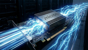
As the calendar turns to January 1, 2026, the artificial intelligence industry has reached a pivotal infrastructure milestone: the definitive end of the "Copper Era" in high-performance data centers. Over the past 18 months, the relentless pursuit of larger Large Language Models (LLMs) and more complex generative agents has pushed traditional electrical networking to its physical breaking point. The solution, long-promised but only recently perfected, is Silicon Photonics—the integration of laser-based data transmission directly into the silicon chips that power AI.
This transition marks a fundamental shift in how AI clusters are built. By replacing copper wires with pulses of light for chip-to-chip communication, the industry has successfully bypassed the "interconnect bottleneck" that threatened to stall the scaling of AI. This development is not merely an incremental speed boost; it is a total redesign of the data center's nervous system, enabling million-GPU clusters to operate as a single, cohesive supercomputer with unprecedented efficiency and bandwidth.
Breaking the Copper Wall: Technical Specifications of the Optical Revolution
The primary driver for this shift is a physical phenomenon known as the "Copper Wall." As data rates reached 224 Gbps per lane in late 2024 and throughout 2025, the reach of passive copper cables plummeted to less than one meter. To send electrical signals any further required massive amounts of power for amplification and retiming, leading to a scenario where interconnects accounted for nearly 30% of total data center energy consumption. Furthermore, "shoreline bottlenecks"—the limited physical space on the edge of a GPU for electrical pins—prevented hardware designers from adding more I/O to match the increasing compute power of the chips.
The technical breakthrough that solved this is Co-Packaged Optics (CPO). In early 2025, Nvidia (NASDAQ: NVDA) unveiled its Quantum-X InfiniBand and Spectrum-X Ethernet platforms, which moved the optical conversion process inside the processor package using TSMC’s (NYSE: TSM) Compact Universal Photonic Engine (COUPE) technology. These systems support up to 144 ports of 800 Gb/s, delivering a staggering 115 Tbps of total throughput. By integrating the laser and optical modulators directly onto the chiplet, Nvidia reduced power consumption by 3.5x compared to traditional pluggable modules, while simultaneously cutting latency from microseconds to nanoseconds.
Unlike previous approaches that relied on external pluggable transceivers, the new generation of Optical I/O, such as Intel’s (NASDAQ: INTC) Optical Compute Interconnect (OCI) chiplet, allows for bidirectional data transfer at 4 Tbps over distances of up to 100 meters. These chiplets operate at just 5 pJ/bit (picojoules per bit), a massive improvement over the 15 pJ/bit required by legacy systems. This allows AI researchers to build "disaggregated" data centers where memory and compute can be physically separated by dozens of meters without sacrificing the speed required for real-time model training.
The Trillion-Dollar Fabric: Market Impact and Strategic Positioning
The shift to Silicon Photonics has triggered a massive realignment among tech giants and semiconductor firms. In a landmark move in December 2025, Marvell (NASDAQ: MRVL) completed its acquisition of startup Celestial AI in a deal valued at over $5 billion. This acquisition gave Marvell control over the "Photonic Fabric," a technology that allows GPUs to access massive pools of external memory with the same speed as if that memory were on the chip itself. This has positioned Marvell as the primary challenger to Nvidia’s dominance in custom AI silicon, particularly for hyperscalers like Amazon (NASDAQ: AMZN) and Meta (NASDAQ: META) who are looking to build their own bespoke AI accelerators.
Broadcom (NASDAQ: AVGO) has also solidified its position by moving into volume production of its Tomahawk 6-Davisson switch. Announced in late 2025, the Tomahawk 6 is the world’s first 102.4 Tbps Ethernet switch featuring integrated CPO. By successfully deploying these switches in Meta's massive AI clusters, Broadcom has proven that silicon photonics can meet the reliability standards required for 24/7 industrial AI operations. This has put immense pressure on traditional networking companies that were slower to pivot away from pluggable optics.
For AI labs like OpenAI and Anthropic, this technological leap means the "scaling laws" can continue to hold. The ability to connect hundreds of thousands of GPUs into a single fabric allows for the training of models with tens of trillions of parameters—models that were previously impossible to train due to the latency of copper-based networks. The competitive advantage has shifted toward those who can secure not just the fastest GPUs, but the most efficient optical fabrics to link them.
A Sustainable Path to AGI: Wider Significance and Concerns
The broader significance of Silicon Photonics lies in its impact on the environmental and economic sustainability of AI. Before the widespread adoption of CPO, the power trajectory of AI data centers was unsustainable, with some estimates suggesting they would consume 10% of global electricity by 2030. Silicon Photonics has bent that curve. By reducing the energy required for data movement by over 60%, the industry has found a way to continue scaling compute power while keeping energy growth manageable.
This transition also marks the realization of "The Rack is the Computer" philosophy. In the past, a data center was a collection of individual servers. Today, thanks to the high-bandwidth, low-latency reach of optical interconnects, an entire rack—or even multiple rows of racks—functions as a single, giant processor. This architectural shift is a prerequisite for the next stage of AI development: distributed reasoning engines that require massive, instantaneous data exchange across thousands of nodes.
However, the shift is not without its concerns. The complexity of manufacturing silicon photonics—which requires the precise alignment of lasers and optical fibers at a microscopic scale—has created a new set of supply chain vulnerabilities. The industry is now heavily dependent on a few specialized packaging facilities, primarily those owned by TSMC and Intel. Any disruption in this specialized supply chain could stall the global rollout of nextgeneration AI infrastructure more effectively than a shortage of raw compute chips.
The Road to 2030: Future Developments in Light-Based Computing
Looking ahead, the next frontier is the "All-Optical Data Center." While we have successfully transitioned the interconnects to light, the actual processing of data still occurs electrically within the transistors. Experts predict that by 2028, we will see the first commercial "Optical Compute" chips from companies like Lightmatter, which use light not just to move data, but to perform the matrix multiplications at the heart of AI workloads. Lightmatter’s Passage M1000 platform, which already supports 114 Tbps of bandwidth, is a precursor to this future.
Near-term developments will focus on reducing power consumption even further, targeting the "sub-1 pJ/bit" threshold. This will likely involve 3D stacking of photonic layers directly on top of logic layers, eliminating the need for any horizontal electrical traces. As these technologies mature, we expect to see Silicon Photonics migrate from the data center into edge devices, enabling high-performance AI in autonomous vehicles and advanced robotics where power and heat are strictly limited.
The primary challenge remaining is the "Laser Problem." Currently, most systems use external laser sources because lasers generate heat that can interfere with sensitive logic circuits. Researchers are working on "quantum dot" lasers that can be grown directly on silicon, which would further simplify the architecture and reduce costs. If successful, this would make Silicon Photonics as ubiquitous as the transistor itself.
Summary: The New Foundation of Artificial Intelligence
The successful integration of Silicon Photonics into the AI stack represents one of the most significant engineering achievements of the 2020s. By breaking the copper wall, the industry has cleared the path for the next generation of AI clusters, moving from the gigabit era into a world of petabit-per-second connectivity. The key takeaways from this transition are the massive gains in power efficiency, the shift toward disaggregated data center architectures, and the consolidation of market power among those who control the optical fabric.
As we move through 2026, the industry will be watching for the first "million-GPU" clusters powered entirely by CPO. These facilities will serve as the proving ground for the most advanced AI models ever conceived. Silicon Photonics has effectively turned the "interconnect bottleneck" from a looming crisis into a solved problem, ensuring that the only limit to AI’s growth is the human imagination—and the availability of clean energy to power the lasers.
This content is intended for informational purposes only and represents analysis of current AI developments.
TokenRing AI delivers enterprise-grade solutions for multi-agent AI workflow orchestration, AI-powered development tools, and seamless remote collaboration platforms.
For more information, visit https://www.tokenring.ai/.


