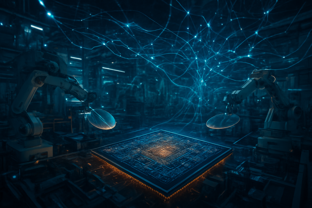
The global semiconductor landscape has reached a pivotal milestone as Taiwan Semiconductor Manufacturing Company (TSMC) (NYSE: TSM) officially entered high-volume manufacturing for its N2 (2nm) technology node. This transition, which began in late 2025 and is ramping up significantly in January 2026, represents the most substantial architectural shift in silicon manufacturing in over a decade. By moving away from the long-standing FinFET design in favor of Gate-All-Around (GAA) nanosheet transistors, TSMC is providing the foundational hardware necessary to sustain the exponential growth of generative AI and high-performance computing (HPC).
As the first N2 chips begin shipping from Fab 20 in Hsinchu, the immediate significance cannot be overstated. This node is not merely an incremental update; it is the linchpin of the "2nm Race," a high-stakes competition between the world’s leading foundries to define the next generation of computing. With power efficiency improvements of up to 30% and performance gains of 15% over the previous 3nm generation, the N2 node is set to become the standard for the next generation of smartphones, data center accelerators, and edge AI devices.
The Technical Leap: Nanosheets and the End of FinFET
The N2 node marks TSMC's departure from the FinFET (Fin Field-Effect Transistor) architecture, which served the industry since the 22nm era. In its place, TSMC has implemented Nanosheet GAAFET technology. Unlike FinFETs, where the gate covers the channel on three sides, the GAA architecture allows the gate to wrap entirely around the channel on all four sides. This provides superior electrostatic control, drastically reducing current leakage and allowing for lower operating voltages. For AI researchers and hardware engineers, this means chips can either run faster at the same power level or maintain current performance while significantly extending battery life or reducing cooling requirements in massive server farms.
Technical specifications for N2 are formidable. Compared to the N3E node (the previous performance leader), N2 offers a 10% to 15% increase in speed at the same power consumption, or a 25% to 30% reduction in power at the same clock speed. Furthermore, chip density has increased by over 15%, allowing designers to pack more logic and memory into the same physical footprint. However, this advancement comes at a steep price; industry insiders report that N2 wafers are commanding a premium of approximately $30,000 each, a significant jump from the $20,000 to $25,000 range seen for 3nm wafers.
Initial reactions from the industry have been overwhelmingly positive regarding yield rates. While architectural shifts of this magnitude are often plagued by manufacturing defects, TSMC's N2 logic test chip yields are reportedly hovering between 70% and 80%. This stability is a testament to TSMC’s "mother fab" strategy at Fab 20 (Baoshan), which has allowed for rapid iteration and stabilization of the complex GAA manufacturing process before expanding to other sites like Kaohsiung’s Fab 22.
Market Dominance and the Strategic Advantages of N2
The rollout of N2 has solidified TSMC's position as the primary partner for the world’s most valuable technology companies. Apple (NASDAQ: AAPL) remains the anchor customer, having reportedly secured over 50% of the initial N2 capacity for its upcoming A20 and M6 series processors. This early access gives Apple a distinct advantage in the consumer market, enabling more sophisticated "on-device" AI features that require high efficiency. Meanwhile, NVIDIA (NASDAQ: NVDA) has reserved significant capacity for its "Feynman" architecture, the anticipated successor to its Rubin AI platform, signaling that the future of large language model (LLM) training will be built on TSMC’s 2nm silicon.
The competitive implications are stark. Intel (NASDAQ: INTC), with its Intel 18A node, is vying for a piece of the 2nm market and has achieved an earlier implementation of Backside Power Delivery (BSPDN). However, Intel’s yields are estimated to be between 55% and 65%, lagging behind TSMC’s more mature production lines. Similarly, Samsung (KRX:005930) began SF2 production in late 2025 but continues to struggle with yields in the 40% to 50% range. While Samsung has garnered interest from companies looking to diversify their supply chains, TSMC's superior yield and reliability make it the undisputed leader for high-stakes, large-scale AI silicon.
This dominance creates a strategic moat for TSMC. By providing the highest performance-per-watt in the industry, TSMC is effectively dictating the roadmap for AI hardware. For startups and mid-tier chip designers, the high cost of N2 wafers may prove a barrier to entry, potentially leading to a market where only the largest "hyperscalers" can afford the most advanced silicon, further concentrating power among established tech giants.
The Geopolitics and Physics of the 2nm Race
The 2nm race is more than just a corporate competition; it is a critical component of the global AI landscape. As AI models become more complex, the demand for "compute" has become a matter of national security and economic sovereignty. TSMC’s success in bringing N2 to market on schedule reinforces Taiwan’s central role in the global technology supply chain, even as the U.S. and Europe attempt to bolster their domestic manufacturing capabilities through initiatives like the CHIPS Act.
However, the transition to 2nm also highlights the growing challenges of Moore’s Law. As transistors approach the atomic scale, the physical limits of silicon are becoming more apparent. The move to GAA is one of the last major structural changes possible before the industry must look toward exotic materials or fundamentally different computing paradigms like photonics or quantum computing. Comparison to previous breakthroughs, such as the move from planar transistors to FinFET in 2011, suggests that each subsequent "jump" is becoming more expensive and technically demanding, requiring billions of dollars in R&D and capital expenditure.
Environmental concerns also loom large. While N2 chips are more efficient, the energy required to manufacture them—including the use of Extreme Ultraviolet (EUV) lithography—is immense. TSMC’s ability to balance its environmental commitments with the massive energy demands of 2nm production will be a key metric of its long-term sustainability in an increasingly carbon-conscious global market.
Future Horizons: Beyond Base N2 to A16
Looking ahead, the N2 node is just the beginning of a multi-year roadmap. TSMC has already announced the N2P (Performance-Enhanced) variant, scheduled for late 2026, which will offer further efficiency gains without the complexity of backside power delivery. The true leap will come with the A16 (1.6nm) node, which will introduce "Super Power Rail" (SPR)—TSMC’s implementation of Backside Power Delivery Network (BSPDN). This technology moves power routing to the back of the wafer, reducing electrical resistance and freeing up more space for signal routing on the front.
Experts predict that the focus of the next three years will shift from mere transistor scaling to "system-level" scaling. This includes advanced packaging technologies like CoWoS (Chip on Wafer on Substrate), which allows N2 logic chips to be tightly integrated with high-bandwidth memory (HBM). As we move toward 2027, the challenge will not just be making smaller transistors, but managing the massive amounts of data flowing between those transistors in AI workloads.
Conclusion: A Defining Chapter in Semiconductor History
TSMC's successful ramp of the N2 node marks a definitive win in the 2nm race. By delivering a stable, high-yield GAA process, TSMC has ensured that the next generation of AI breakthroughs will have the hardware foundation they require. The transition from FinFET to Nanosheet is more than a technical footnote; it is the catalyst for the next era of high-performance computing, enabling everything from real-time holographic communication to autonomous systems with human-level reasoning.
In the coming months, all eyes will be on the first consumer products powered by N2. If these chips deliver the promised efficiency gains, it will spark a massive upgrade cycle in both the consumer and enterprise sectors. For now, TSMC remains the king of the foundry world, but with Intel and Samsung breathing down its neck, the race toward 1nm and beyond is already well underway.
This content is intended for informational purposes only and represents analysis of current AI developments.
TokenRing AI delivers enterprise-grade solutions for multi-agent AI workflow orchestration, AI-powered development tools, and seamless remote collaboration platforms.
For more information, visit https://www.tokenring.ai/.