The HBM Arms Race: SK Hynix Greenlights $13 Billion Packaging Mega-Fab to Anchor the HBM4 Era
In a move that underscores the insatiable demand for artificial intelligence hardware, SK Hynix (KRX: 000660) has officially approved a staggering $13 billion (19 trillion won) investment to construct the world’s largest High Bandwidth Memory (HBM) packaging facility. Known as P&T7 (Package & Test 7), the plant will be located in the Cheongju Technopolis Industrial Complex in South Korea. This monumental capital expenditure, announced as the industry gathers for the start of 2026, marks a pivotal moment in the global semiconductor race, effectively doubling down on the infrastructure required to move from the current HBM3e standard to the next-generation HBM4 architecture.
The significance of this investment cannot be overstated. As AI clusters like Microsoft (NASDAQ: MSFT) and OpenAI’s "Stargate" and xAI’s "Colossus" scale to hundreds of thousands of GPUs, the memory bottleneck has become the primary constraint for large language model (LLM) performance. By vertically integrating the P&T7 packaging plant with its adjacent M15X DRAM fab, SK Hynix aims to streamline the production of 12-layer and 16-layer HBM4 stacks. This "organic linkage" is designed to maximize yields and minimize latency, providing the specialized memory necessary to feed the data-hungry Blackwell Ultra and Vera Rubin architectures from NVIDIA (NASDAQ: NVDA).
Technical Leap: Moving Beyond HBM3e to HBM4
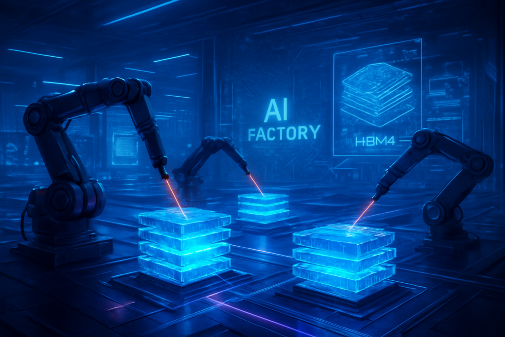
The transition from HBM3e to HBM4 represents the most significant architectural shift in memory technology in a decade. While HBM3e utilized a 1024-bit interface, HBM4 doubles this to a 2048-bit interface, effectively widening the data highway to support bandwidths exceeding 2 terabytes per second (TB/s). SK Hynix recently showcased a world-first 48GB 16-layer HBM4 stack at CES 2026, utilizing advanced "Advanced MR-MUF" (Mass Reflow Molded Underfill) technology to manage the heat generated by such dense vertical stacking.
Unlike previous generations, HBM4 will also see the introduction of "semi-custom" logic dies. For the first time, memory vendors are collaborating directly with foundries like TSMC (NYSE: TSM) to manufacture the base die of the memory stack using logic processes rather than traditional memory processes. This allows for higher efficiency and better integration with the host GPU or AI accelerator. Industry experts note that this shift essentially turns HBM from a commodity component into a bespoke co-processor, a move that requires the precise, large-scale packaging capabilities that the new $13 billion Cheongju facility is built to provide.
The Big Three: Samsung and Micron Fight for Dominance
While SK Hynix currently commands approximately 60% of the HBM market, its rivals are not sitting idle. Samsung Electronics (KRX: 005930) is aggressively positioning its P5 fab in Pyeongtaek as a primary HBM4 volume base, with the company aiming for mass production by February 2026. After a slower start in the HBM3e cycle, Samsung is betting big on its "one-stop" shop advantage, offering foundry, logic, and memory services under one roof—a strategy it hopes will lure customers looking for streamlined HBM4 integration.
Meanwhile, Micron Technology (NASDAQ: MU) is executing its own global expansion, fueled by a $7 billion HBM packaging investment in Singapore and its ongoing developments in the United States. Micron’s HBM4 samples are already reportedly reaching speeds of 11 Gbps, and the company has reached an $8 billion annualized revenue run-rate for HBM products. The competition has reached such a fever pitch that major customers, including Meta (NASDAQ: META) and Google (NASDAQ: GOOGL), have already pre-allocated nearly the entire 2026 production capacity for HBM4 from all three manufacturers, leading to a "sold out" status for the foreseeable future.
AI Clusters and the Capacity Penalty
The expansion of these packaging plants is directly tied to the exponential growth of AI clusters, a trend highlighted in recent industry reports as the "HBM3e to HBM4 migration." As specified in Item 3 of the industry’s top 25 developments for 2026, the reliance on HBM4 is now a prerequisite for training next-generation models like Llama 4. These massive clusters require memory that is not only faster but also significantly denser to handle the trillion-parameter counts of future frontier models.
However, this focus on HBM comes with a "capacity penalty" for the broader tech industry. Manufacturing HBM4 requires nearly three times the wafer area of standard DDR5 DRAM. As SK Hynix and its peers pivot their production lines to HBM to meet AI demand, a projected 60-70% shortage in standard DDR5 modules is beginning to emerge. This shift is driving up costs for traditional data centers and consumer PCs, as the world’s most advanced fabrication equipment is increasingly diverted toward specialized AI memory.
The Horizon: From HBM4 to HBM4E and Beyond
Looking ahead, the roadmap for 2027 and 2028 points toward HBM4E, which will likely push stacking to 20 or 24 layers. The $13 billion SK Hynix plant is being built with these future iterations in mind, incorporating cleanroom standards that can accommodate hybrid bonding—a technique that eliminates the use of traditional solder bumps between chips to allow for even thinner, more efficient stacks.
Experts predict that the next two years will see a "localization" of the supply chain, as SK Hynix’s Indiana plant and Micron’s New York facilities come online to serve the U.S. domestic AI market. The challenge for these firms will be maintaining high yields in an increasingly complex manufacturing environment where a single defect in one of the 16 layers can render an entire $500+ HBM stack useless.
Strategic Summary: Memory as the New Oil
The $13 billion investment by SK Hynix marks a definitive end to the era where memory was an afterthought in the compute stack. In the AI-driven economy of 2026, memory has become the "new oil," the essential fuel that determines the ceiling of machine intelligence. As the Cheongju P&T7 facility begins construction this April, it serves as a physical monument to the industry's belief that the AI boom is only in its early chapters.
The key takeaway for the coming months will be how quickly Samsung and Micron can narrow the yield gap with SK Hynix as HBM4 mass production begins. For AI labs and cloud providers, securing a stable supply of this specialized memory will be the difference between leading the AGI race or being left behind. The battle for HBM supremacy is no longer just a corporate rivalry; it is a fundamental pillar of global technological sovereignty.
This content is intended for informational purposes only and represents analysis of current AI developments.
TokenRing AI delivers enterprise-grade solutions for multi-agent AI workflow orchestration, AI-powered development tools, and seamless remote collaboration platforms.
For more information, visit https://www.tokenring.ai/.