As of December 23, 2025, the global race for artificial intelligence supremacy has shifted from a battle over transistor counts to a desperate scramble for physical space and thermal relief. While the industry spent the last decade focused on shrinking logic gates, the primary constraints of 2025 are no longer the chips themselves, but how they are tied together and kept from melting. Advanced packaging—specifically TSMC’s Chip-on-Wafer-on-Substrate (CoWoS) technology—and the looming "thermal wall" have emerged as the twin gatekeepers of AI progress, dictating which companies can ship products and which data centers can stay online.
This shift represents a fundamental change in semiconductor economics. For giants like Nvidia (NASDAQ: NVDA) and AMD (NASDAQ: AMD), the challenge is no longer just designing the world’s most powerful GPU; it is securing a spot in the highly specialized "backend" factories where these chips are assembled into massive, multi-die systems. As power densities reach unprecedented levels, the industry is simultaneously undergoing a forced migration toward liquid cooling, a transition that is minting new winners in the infrastructure space while threatening to leave air-cooled legacy facilities in the dust.
The Technical Frontier: CoWoS-L and the Rise of the 'Silicon Skyscraper'
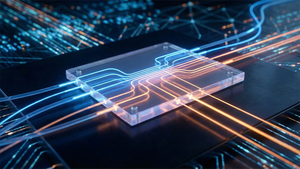
At the heart of the current supply bottleneck is TSMC (NYSE: TSM) and its proprietary CoWoS technology. In 2025, the industry has transitioned heavily toward CoWoS-L (Local Silicon Interconnect), a sophisticated packaging method that uses tiny silicon bridges to link multiple compute dies and High Bandwidth Memory (HBM) modules. This approach allows Nvidia’s Blackwell and the upcoming Rubin architectures to function as a single, massive processor, bypassing the physical size limits of traditional chip manufacturing. By the end of 2025, TSMC is expected to reach a monthly CoWoS capacity of 75,000 to 80,000 wafers—nearly double its 2024 output—yet demand from hyperscalers continues to outpace this expansion.
Technical specifications for these next-gen accelerators have pushed packaging to its breaking point. Current AI chips are now exceeding the "reticle limit," the maximum size a single chip can be printed on a wafer. To solve this, engineers are stacking chips vertically and horizontally, creating what industry experts call "silicon skyscrapers." However, this density introduces a phenomenon known as Coefficient of Thermal Expansion (CTE) mismatch. When these multi-layered stacks heat up, different materials—silicon, organic substrates, and solder—expand at different rates. In early 2025, this led to significant yield challenges for high-end GPUs, as microscopic cracks formed in the interconnects, forcing a redesign of the substrate layers to ensure structural integrity under extreme heat.
Initial reactions from the AI research community have been a mix of awe and concern. While these packaging breakthroughs have enabled a 30x increase in inference performance for large language models, the complexity of the manufacturing process has created a "tiered" AI market. Only the largest tech companies can afford the premium for CoWoS-allocated chips, leading to a widening gap between the "compute-rich" and the "compute-poor." Researchers at leading labs note that while the logic is faster, the latency involved in moving data across these complex packaging interconnects remains the final frontier for optimizing model training.
Market Impact: The New Power Brokers of the AI Supply Chain
The scarcity of advanced packaging has reshaped the competitive landscape, turning backend assembly into a strategic weapon. While TSMC remains the undisputed leader, the sheer volume of demand has forced a new "split manufacturing" model. TSMC now focuses on the high-margin "Chip-on-Wafer" (CoW) stage, while outsourcing the "on Substrate" (oS) assembly to Outsourced Semiconductor Assembly and Test (OSAT) providers. This has been a massive boon for companies like ASE Technology (NYSE: ASX) and Amkor Technology (NASDAQ: AMKR), which have become essential partners for Nvidia and AMD. ASE, in particular, has seen its specialized facilities in Taiwan become dedicated extensions of the Nvidia supply chain, handling the final assembly for the Blackwell B200 and GB200 systems.
For the major AI labs, this bottleneck has necessitated a shift in strategy. Microsoft (NASDAQ: MSFT), Google (NASDAQ: GOOGL), and Amazon (NASDAQ: AMZN) are no longer just competing on software; they are increasingly designing their own custom AI silicon (ASICs) to bypass the standard GPU queues. However, even these custom chips require CoWoS packaging, leading to a "co-opetition" where tech giants must negotiate for packaging capacity alongside their primary rivals. This has given TSMC unprecedented pricing power and a strategic advantage that some analysts believe will persist through 2027, as new facilities like AP8 in Tainan only begin to reach full scale in late 2025.
The Thermal Wall: Liquid Cooling Becomes Mandatory
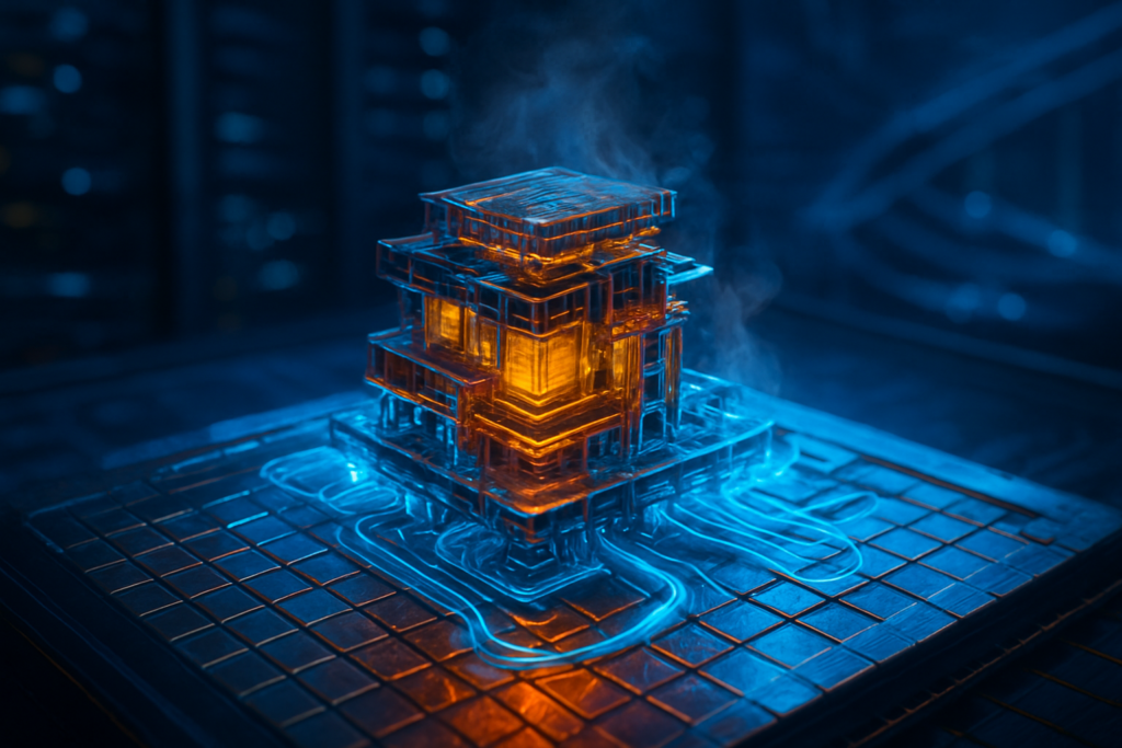
As chip designs become denser, the industry has hit the "thermal wall." In 2025, top-tier AI accelerators are reaching Thermal Design Power (TDP) ratings of 1,200W to 2,700W per module. At these levels, traditional air cooling is physically incapable of dissipating heat fast enough to prevent the silicon from throttling or sustaining permanent damage. This has triggered a massive infrastructure pivot: liquid cooling is no longer an exotic option for enthusiasts; it is a mandatory requirement for AI data centers. Direct-to-Chip (D2C) cooling, where liquid-filled cold plates sit directly on the processor, has become the standard for the newest Nvidia GB200 NVL72 racks.
This transition has catapulted infrastructure companies into the spotlight. Vertiv (NYSE: VRT) and Delta Electronics have seen record growth as they race to provide the Coolant Distribution Units (CDUs) and manifolds required to manage the heat of 100kW+ server racks. The wider significance of this shift cannot be overstated; it represents the end of the "air-cooled era" of computing. Data center operators are now forced to retrofit old facilities with liquid piping—a costly and complex endeavor—or build entirely new "AI Factories" from the ground up. This has also raised environmental concerns, as the massive power requirements of these liquid-cooled clusters place immense strain on regional power grids, leading to a surge in interest for small modular reactors (SMRs) to power the next generation of AI hubs.
Future Horizons: Microfluidics and 3D Integration
Looking ahead to 2026 and 2027, the industry is exploring even more radical solutions to the packaging and thermal dilemmas. One of the most promising developments is microfluidic cooling, where cooling channels are etched directly into the silicon or the interposer itself. By bringing the coolant within micrometers of the heat-generating transistors, researchers believe they can handle power densities exceeding 3kW per chip. Microsoft and TSMC are reportedly already testing these "in-chip" cooling systems for future iterations of the Maia accelerator series, which could potentially reduce thermal resistance by 15% compared to current cold-plate technology.
Furthermore, the move toward 3D IC (Integrated Circuit) stacking—where logic is stacked directly on top of logic—will require even more advanced thermal management. Experts predict that the next major milestone will be the integration of optical interconnects directly into the package. By using light instead of electricity to move data between chips, manufacturers can significantly reduce the heat generated by traditional copper wiring. However, the challenge of aligning lasers with sub-micron precision within a mass-produced package remains a significant hurdle that the industry is racing to solve by the end of the decade.
Summary and Final Thoughts
The developments of 2025 have made one thing clear: the future of AI is as much a feat of mechanical and thermal engineering as it is of computer science. The CoWoS bottleneck has demonstrated that even the most brilliant algorithms are at the mercy of physical manufacturing capacity. Meanwhile, the "thermal wall" has forced a total reimagining of data center architecture, moving the industry toward a liquid-cooled future that was once the stuff of science fiction.
As we look toward 2026, the key indicators of success will be the ramp-up of TSMC’s AP8 and AP7 facilities and the ability of OSATs like Amkor and ASE to take on more complex packaging roles. For investors and industry observers, the focus should remain on the companies that bridge the gap between silicon and the physical world. The AI revolution is no longer just in the cloud; it is in the pipes, the pumps, and the microscopic bridges of the world’s most advanced packages.
This content is intended for informational purposes only and represents analysis of current AI developments.
TokenRing AI delivers enterprise-grade solutions for multi-agent AI workflow orchestration, AI-powered development tools, and seamless remote collaboration platforms.
For more information, visit https://www.tokenring.ai/.