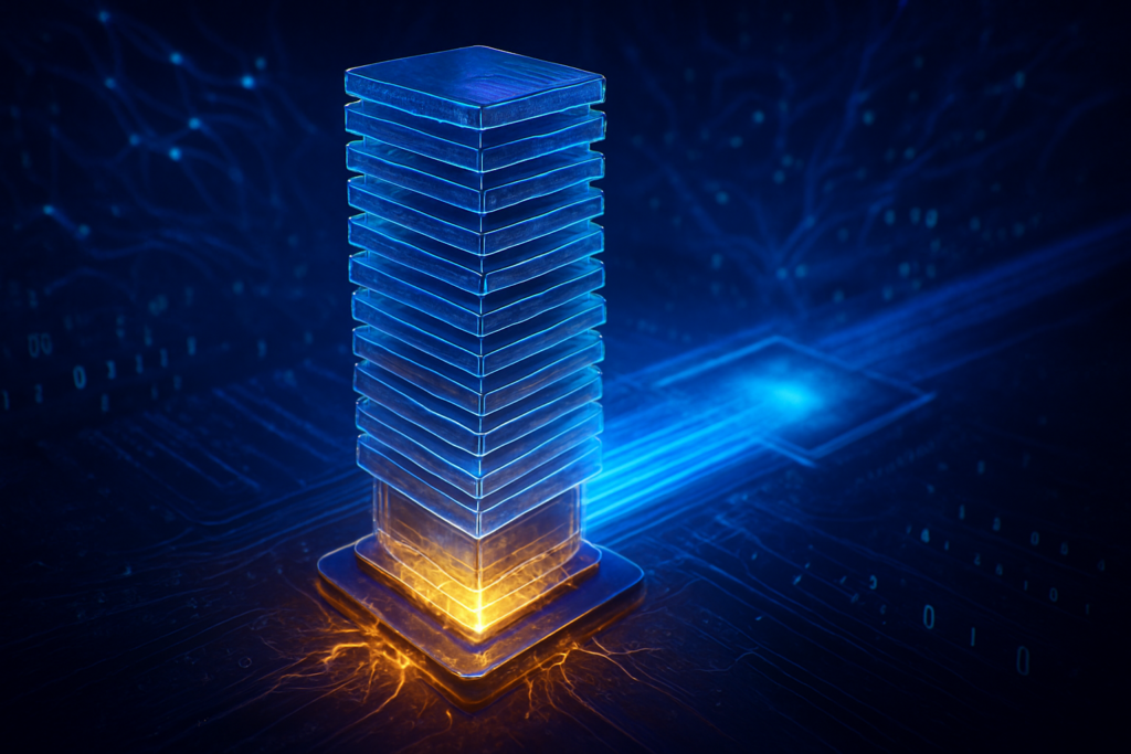
The global race for artificial intelligence supremacy has officially moved beyond the GPU and into the very architecture of memory. As of January 22, 2026, the "Big Three" memory manufacturers—SK Hynix (KOSPI: 000660), Samsung Electronics (KOSPI: 005930), and Micron Technology (NASDAQ: MU)—have all confirmed the delivery of 16-layer (16-Hi) High Bandwidth Memory 4 (HBM4) samples to NVIDIA (NASDAQ: NVDA). This milestone marks a critical shift in the AI infrastructure landscape, transitioning from the incremental improvements of the HBM3e era to a fundamental architectural redesign required to support the next generation of "Rubin" architecture GPUs and the trillion-parameter models they are destined to run.
The immediate significance of this development cannot be overstated. By moving to a 16-layer stack, memory providers are effectively doubling the data "bandwidth pipe" while drastically increasing the memory density available to a single processor. This transition is widely viewed as the primary solution to the "Memory Wall"—the performance bottleneck where the processing power of modern AI chips far outstrips the ability of memory to feed them data. With these 16-Hi samples now undergoing rigorous qualification by NVIDIA, the industry is bracing for a massive surge in AI training efficiency and the feasibility of 100-trillion parameter models, which were previously considered computationally "memory-bound."
Breaking the 1024-Bit Barrier: The Technical Leap to HBM4
HBM4 represents the most significant architectural overhaul in the history of high-bandwidth memory. Unlike previous generations that relied on a 1024-bit interface, HBM4 doubles the interface width to 2048-bit. This "wider pipe" allows for aggregate bandwidths exceeding 2.0 TB/s per stack. To meet NVIDIA’s revised "Rubin-class" specifications, these 16-Hi samples have been engineered to achieve per-pin data rates of 11 Gbps or higher. This technical feat is achieved by stacking 16 individual DRAM layers—each thinned to roughly 30 micrometers, or one-third the thickness of a human hair—within a JEDEC-mandated height of 775 micrometers.
The most transformative technical change, however, is the integration of the "logic die." For the first time, the base die of the memory stack is being manufactured on high-performance foundry nodes rather than standard DRAM processes. SK Hynix has partnered with Taiwan Semiconductor Manufacturing Co. (NYSE: TSM) to produce these base dies using 12nm and 5nm nodes. This allows for "active memory" capabilities, where the memory stack itself can perform basic data pre-processing, reducing the round-trip latency to the GPU. Initial reactions from the AI research community suggest that this integration could improve energy efficiency by 30% and significantly reduce the heat generation that plagued early 12-layer HBM3e prototypes.
The shift to 16-Hi stacks also enables unprecedented VRAM capacities. A single NVIDIA Rubin GPU equipped with eight 16-Hi HBM4 stacks can now boast between 384GB and 512GB of total VRAM. This capacity is essential for the inference of massive Large Language Models (LLMs) that previously required entire clusters of GPUs just to hold the model weights in memory. Industry experts have noted that the 16-layer transition was "the hardest in HBM history," requiring advanced packaging techniques like Mass Reflow Molded Underfill (MR-MUF) and, in Samsung’s case, the pioneering of copper-to-copper "hybrid bonding" to eliminate the need for micro-bumps between layers.
The Tri-Polar Power Struggle: Market Positioning and Strategic Advantages
The delivery of these samples has ignited a fierce competitive struggle for dominance in NVIDIA's lucrative supply chain. SK Hynix, currently the market leader, utilized CES 2026 to showcase a functional 48GB 16-Hi HBM4 package, positioning itself as the "frontrunner" through its "One Team" alliance with TSMC. By outsourcing the logic die to TSMC, SK Hynix has ensured its memory is perfectly "tuned" for the CoWoS (Chip-on-Wafer-on-Substrate) packaging that NVIDIA uses for its flagship accelerators, creating a formidable barrier to entry for its competitors.
Samsung Electronics, meanwhile, is pursuing an "all-under-one-roof" turnkey strategy. By using its own 4nm foundry process for the logic die and its proprietary hybrid bonding technology, Samsung aims to offer NVIDIA a more streamlined supply chain and potentially lower costs. Despite falling behind in the HBM3e race, Samsung's aggressive acceleration to 16-Hi HBM4 is a clear bid to reclaim its crown. However, reports indicate that Samsung is also hedging its bets by collaborating with TSMC to ensure its 16-Hi stacks remain compatible with NVIDIA’s standard manufacturing flows.
Micron Technology has carved out a unique position by focusing on extreme energy efficiency. At CES 2026, Micron confirmed that its HBM4 capacity for the entirety of 2026 is already "sold out" through advance contracts, despite its mass production slated for slightly later than SK Hynix. Micron’s strategy targets the high-volume inference market where power costs are the primary concern for hyperscalers. This three-way battle ensures that while NVIDIA remains the primary gatekeeper, the diversity of technical approaches—SK Hynix’s partnership model, Samsung’s vertical integration, and Micron’s efficiency focus—will prevent a single-supplier monopoly from forming.
Beyond the Hardware: Implications for the Global AI Landscape
The arrival of 16-Hi HBM4 marks a pivotal moment in the broader AI landscape, moving the industry toward "Scale-Up" architectures where a single node can handle massive workloads. This fits into the trend of "Trillion-Parameter Scaling," where the size of AI models is no longer limited by the physical space on a motherboard but by the density of the memory stacks. The ability to fit a 100-trillion parameter model into a single rack of Rubin-powered servers will drastically reduce the networking overhead that currently consumes up to 30% of training time in modern data centers.
However, the wider significance of this development also brings concerns regarding the "Silicon Divide." The extreme cost and complexity of HBM4—which is reportedly five to seven times more expensive than standard DDR5 memory—threaten to widen the gap between tech giants like Microsoft (NASDAQ: MSFT) or Google (NASDAQ: GOOGL) and smaller AI startups. Furthermore, the reliance on advanced packaging and logic die integration makes the AI supply chain even more dependent on a handful of facilities in Taiwan and South Korea, raising geopolitical stakes. Much like the previous breakthroughs in Transformer architectures, the HBM4 milestone is as much about economic and strategic positioning as it is about raw gigabytes per second.
The Road to HBM5 and Hybrid Bonding: What Lies Ahead
Looking toward the near-term, the focus will shift from sampling to yield optimization. While SK Hynix and Samsung have delivered 16-Hi samples, the challenge of maintaining high yields across 16 layers of thinned silicon is immense. Experts predict that 2026 will be a year of "Yield Warfare," where the company that can most reliably produce these stacks at scale will capture the majority of NVIDIA's orders for the Rubin Ultra refresh expected in 2027.
Beyond HBM4, the horizon is already showing signs of HBM5, which is rumored to explore 20-layer and 24-layer stacks. To achieve this without exceeding the physical height limits of GPU packages, the industry must fully transition to hybrid bonding—a process that fuses copper pads directly together without any intervening solder. This transition will likely turn memory makers into "semi-foundries," further blurring the line between storage and processing. We may soon see "Custom HBM," where AI labs like OpenAI or Anthropic design their own logic dies to be placed at the bottom of the memory stack, specifically optimized for their unique neural network architectures.
Wrapping Up the HBM4 Revolution
The delivery of 16-Hi HBM4 samples to NVIDIA by SK Hynix, Samsung, and Micron marks the end of memory as a simple commodity and the beginning of its era as a custom logic component. This development is arguably the most significant hardware milestone of early 2026, providing the necessary bandwidth and capacity to push AI models past the 100-trillion parameter threshold. As these samples move into the qualification phase, the success of each manufacturer will be defined not just by speed, but by their ability to master the complex integration of logic and memory.
In the coming weeks and months, the industry should watch for NVIDIA’s official qualification results, which will determine the initial allocation of "slots" on the Rubin platform. The battle for HBM4 dominance is far from over, but the opening salvos have been fired, and the stakes—control over the fundamental building blocks of the AI era—could not be higher. For the technology industry, the HBM4 era represents the definitive breaking of the "Memory Wall," paving the way for AI capabilities that were, until now, strictly theoretical.
This content is intended for informational purposes only and represents analysis of current AI developments.
TokenRing AI delivers enterprise-grade solutions for multi-agent AI workflow orchestration, AI-powered development tools, and seamless remote collaboration platforms.
For more information, visit https://www.tokenring.ai/.